From the September edition of pv magazine
Philipp Matter from GCL Systems Integration says that only a few years ago, he did not have a precise understanding of module dimensions. “They were all the same.” Today, Matter says, things are different. “It’s a bit of a mess, but it’s part of the proceedings and the improvement of technology, so we have to take it.”
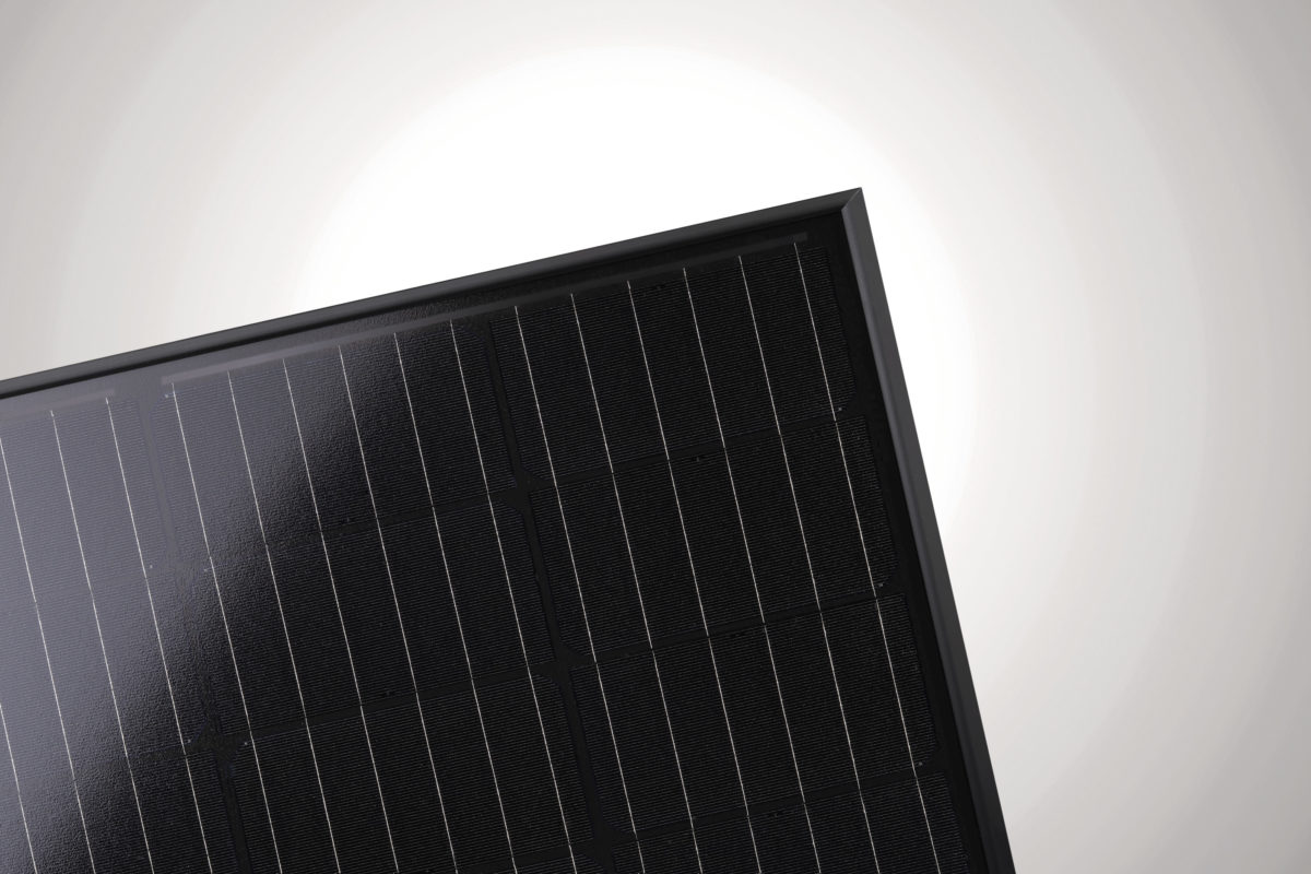
Over the past decade, the size of silicon wafers for the solar industry has slowly crept upward. Larger wafers offer the potential for savings in production, but for the most part, changes have been slow and incremental, as there is a need to minimize disruption to the downstream industry. Major changes to the size of this key component could necessitate an expensive overhaul of cell and module production lines, while also affecting installation practices, racking design and other balance-of-systems components.
From around 2010, suppliers began to move to 156 mm² as a standard size, and older 125 mm² wafers were more or less eliminated from the market by 2014. Wafer suppliers in China then adopted 156.75 mm² as a standard, and this became the M2 wafer format, which the International Technology Roadmap for Photovoltaics says represented more than 90% of the market for both mono- and multicrystalline wafers in 2018.
Scaling up
In 2019, manufacturers have again begun to diverge from this standard, as they look to maximize active space in the module to meet the industry’s demand for consistently higher power ratings. Several major manufacturers have launched modules based on wafers measuring 158.75 mm², while a handful of high-efficiency suppliers are working with the M4 format, measuring 161.75 mm².
And it doesn’t stop there. In June, leading wafer supplier Longi Green Energy Technology launched its new M6 wafer, measuring 166 mm². And in August, Zhonghuan Semiconductor took the trend to another level when it launched the supersized “Kwafoo” wafer, measuring 210 mm².
The rationale behind any increase in wafer size is reduced costs. In production, the aim is to produce the larger format at the same level of throughput, effecting a reduction in the cost per watt. And further down the line, the goal is to reduce balance of systems costs by fitting more watts into the same size racking system.
According to Longi, the M6 wafer has an area 12.2% larger than the M2, providing an 8.8% boost to power output. Back in May, Longi launched the M6 at CNY 3.47 ($0.49) per piece, and the price has since remained slightly above that of the smaller M2. Longi has stated, however, that with its economies of scale it expects to reduce the price premium to less than CNY 0.20 per piece.
The company estimates that its new M6 wafer brings down costs at the cell and module level by around $0.007/W, while also reducing the spend on other components including racking, foundations and cabling by around $0.01/W.
“With a larger module size, each array requires fewer brackets, and each bracket requires more steel in order to carry a larger module,” explains a Longi spokesperson. “But this cost increase is lower than the bracket decrease. Therefore, the bracket cost is reduced, and the number of pile foundations is generally proportional to the number of brackets. Therefore, the cost decreases significantly with the increase of module power.”
Varying sizes
With at least three different wafer sizes gaining ground commercially, it is difficult to say which, if any, will form a new standard. Longi is keen to promote its M6 as the best option. “With this size, there is no need to replace the tube furnace. And a bifacial module using 2 mm glass+frame weighs less than 30 kg, and still can be handled and installed by two people,” says the Longi spokesperson. “A smaller increase will still change the module size and require all new certifications. Therefore, Longi believes that if the wafer size should be changed,
166 mm is the right choice.”
Other manufacturers appear to have settled on 158.75 mm² as the optimal size to offer the best compromise between manufacturing processes and module features. GCL Systems Integration stated earlier this year that it would work with this size in all future projects. Last year, JinkoSolar also brought its Cheetah series to the market and has now shipped more than 5 GW of products that incorporate the wafer.
“We have done our homework on this and we think we understand that this [158.75 mm] is the right size for the industry at the moment,” said Gener Miao, JinkoSolar’s VP for global sales and marketing. “With even larger sizes we have done the research and this would create a lot of disruption. You would have to design a whole new racking system. As a manufacturer we can do larger wafers, but I don’t think the downstream sector is ready for it.”
And in between these two is the M4 wafer, measuring 161.7mm. It has been available for several years, and has been mainly adopted by manufacturers offering premium high-efficiency products, including Hanwha Q Cells, REC Group, LG and SunPower. “We opted for M4 wafers with an edge length of 161.7 mm as the most cost-effective choice in the market,” says Jürgen Steinberger, manager of Q Cells Product Management. “M4 wafers make better use of the ingot than M2 wafers, help increase module power by 20 to 25 watts, and thus support material and labor cost reduction during installation.”
Maximum output
On the manufacturing side, where players are looking to larger wafers to maximize their module output and get the most out of their investment in machinery, it would make sense to move directly to the largest size that can be processed without major adjustments to the production line. “Adopting a wafer size such as 158.75 mm, which is only marginally larger than M2, does not offer enough LCOE benefit for our customers in order to justify the slight increase in module size,” says Steinberger. “The fact that some of our competitors decided differently suggests that their existing production equipment does not support the use of M4 wafers.”
Longi is keen to stress that its M6 wafer can be adopted on production lines with minimal disruption, and is already seeing widespread acceptance. “The monocrystalline furnace has plenty of room to produce thicker silicon ingots,” says the Longi spokesperson. “Newer cell and module production lines only need replacement of jigs and fixtures, and the cost of transformation is not high. New factories do not need transformation, and will all take the compatibility with M6 wafers into account.”
Suppliers that have opted for the smaller increase to 158.75 mm², however, are keen to stress that minimizing changes to the module dimensions is a key consideration, as it avoids added costs in installation. “We chose the 158.75 mm wafer to lean in toward our EPC partners. This led us to maximizing the wafer size without changing the module dimensions significantly. It’s not a case of ‘the bigger the better’. The target is to optimize the cell size also considering the downstream industry” says Andrea Viaro, head of technical service for Europe at JinkoSolar. “The Cheetah module is just a few centimeters longer and larger, and that’s it; it does not generate extra requirements or costs to adapt the PV array configuration. We have done much research, and with larger sizes the design of the system would create a lot of disruption.”
With its announcement of the 210mm² Kwafoo wafer, however, China’s Zhonghuan Semiconductor looks to be inviting this type of disruption. The company says a 120 half-cell PERC module incorporating the wafer could achieve a power rating of 610 W. However, this would surely mean a much larger form factor – one that would likely make big investments in new production equipment a necessity, as well as complete redesigns at the system level. Zhonghuan Chairman Shen Haoping, however, is convinced of the Kwafoo wafer’s potential to reduce project costs. The company says it will now “work closely with partners from the entire value chain to build up a lower cost and more efficient platform for the solar PV market,” which may be more of a long-term goal, given the implications for customers of the new larger wafer.
“The much larger 210 mm wafer format poses some challenges along the supply chain,” says Steinberger. “Such large wafers do appear promising – especially for lowering capex per watt for manufacturing tools, from ingot to cell – but even slight negative effects on production yields or cell efficiencies could easily cancel out such benefits.”
With multiple wafer sizes in use – not to mention different choices regarding the number of cells and their layout in a module – there are conflicting theories as to where the sweet spot lies between cost optimizations in module manufacturing and added weight or complexity in installation. And in practice as well, this will likely vary depending upon project specific parameters.
“The industry is now determining how to balance the equation,” says Eduardo de San Nicolás, sales coordinator and product director at tracker manufacturer Soltec. “As panels grow in size, at some point, the upfront manufacturing savings of the larger panels will offset the extra cost of reinforced structures and BOS construction.”
Differentiation vs. standardization
Differentiation has emerged as a major trend among module makers in recent years, as they look to make their offerings stand out in a crowded marketplace, and as technologies grow more tailored to specific applications.
Applying this to wafer size, it could be that the different sizes coming to the market are each able to find their niche – for example, many rooftops would be unable to accommodate larger, heavier modules, while ground-mount racking systems can be reinforced relatively easily.
“In the last years, module makers have introduced a variety of types of cells, frames, and technologies, thus making it harder to standardize,” continues San Nicolás. “We cannot foresee a module dimension standardization in the industry in the short- nor the mid-term. Instead, the market is putting its efforts into a seamless panel-tracker integration that minimizes installation costs.”
Cell and module manufacturers, however, have been more vocal in calling for standardization as a way to keep driving costs down. “The potential risk that we see with diversified module sizes on the market is an increase in the mismatches along the supply chain,” says JinkoSolar’s Viaro. “This might create complexity, and ultimately higher costs for the end customer.”
Longi has also called for manufacturers to adopt the M6 wafer as an industry standard. “A standard size can help the whole industry reduce costs and avoid frequent changes in the product specifications,” says the spokesperson, noting that the M6 wafer will be its main direction in the future, even though there is still demand for the M2.
For now, research and collaboration are needed to balance the needs of manufacturers with those of their customers. What’s certain is that we won’t see the market accepting lower power ratings. And since a larger wafer is a relatively simple way to push more watts out at module level, this is likely the way the industry will move – and the M2 format could soon be a thing of the past.
Whether increasing to 158.75 mm, 161 mm, 166 mm or even larger will prove the optimal strategy here remains a question the industry will soon need to answer. “There is a theoretical tipping point in which the savings in terms of Wp derived from manufacturing larger panels will not be able to balance the higher costs of manufacturing larger trackers and handling bigger and heavier panels of a PV plant’s construction,” says Soltec’s de San Nicolás. “We are collaborating with EPC contractors and panel manufacturers to determine that threshold.”
This content is protected by copyright and may not be reused. If you want to cooperate with us and would like to reuse some of our content, please contact: editors@pv-magazine.com.


By submitting this form you agree to pv magazine using your data for the purposes of publishing your comment.
Your personal data will only be disclosed or otherwise transmitted to third parties for the purposes of spam filtering or if this is necessary for technical maintenance of the website. Any other transfer to third parties will not take place unless this is justified on the basis of applicable data protection regulations or if pv magazine is legally obliged to do so.
You may revoke this consent at any time with effect for the future, in which case your personal data will be deleted immediately. Otherwise, your data will be deleted if pv magazine has processed your request or the purpose of data storage is fulfilled.
Further information on data privacy can be found in our Data Protection Policy.