From pv magazine 05/2022
The latest International Technology Roadmap for Photovoltaic (ITRPV) report came out in April, and tandem and IBC [interdigitated back contact] cells were forecast to account for 5% of global production capacity by 2032. As a high-efficiency PV equipment supplier, what do you make of that figure?
We consider this as a reasonable number. In China alone there is 300 GW of production capacity today and we believe this will increase, not only in China but also throughout the world. So, even though 5% might seem like a small number, it is a reasonably high number for a relatively new technology – especially if you consider that it is at the R&D or pilot phase, depending on the customer. And as we know from recent developments for heterojunction (HJT) or even PERC in the past, it took a while until production was really at gigawatt scale.
You mentioned some customers on tandem cell production – can you give me an overview of the level of maturity of these manufacturers and their technologies?
It really is a broad range. There are customers that are in an R&D phase, and the watt-scale. Their main purpose is to scale it from centimetre-square solar cells to single-wafer cell, and that is their R&D approach. But others are already beyond this. These companies are already producing on the pilot scale and seriously working on bringing this technology to gigawatt scale.
As an equipment manufacturer, we consider ourselves as a partner for these manufacturers scaling up – from lab, to medium, and then to gigawatt scale. To give you some numbers, when you are talking about a lab tool, it is about 10 wafers per day. When we go to pilot tools, it is 1,000 wafers per day. And then mass production is in multi-megawatt and then gigawatts. Although there are no tandem cell gigawatt producers yet in the market.
Are the partners you are working with mainly in Europe?
In Europe mainly, but also in the United States, and in the Asian region, too.
For these prospective manufacturers, how would you describe the challenges they are facing on the technological level? We know about stability being a major challenge with perovskite tandems – is that still the primary challenge?
It is one of the biggest, but the scaling itself is already a challenge – to scale the technology and all of the process steps and take that into production. The efficiency and stable efficiency is the other one. And the availability and cost of the raw materials must also be considered if a manufacturer is thinking about going into gigawatt production.
And by material development, what do you mean?
The perovskite itself. Perovskite is a material group, and it does have massive advantages in that you can adapt the optical properties – meaning the band gap can be aligned depending on the structure underneath it, to the underlying cell. Usually, perovskites are being applied in tandem devices, with either a silicon or thin film-based cell. And then the optical properties of perovskite can be adapted to deliver high efficiencies. And the other big advantage of perovskite is the cost-efficient synthesis and the production of the material itself.
So, while perovskite materials can be cost effective, getting the material composition itself is a challenge for the developers.
Material selection is a challenge right now, not just for long term stability as you mention, but also for ecological sustainability – which is more and more important. And of course, at the end of the day, the cost. But the potential for low-cost materials with the perovskite group is tremendous.
By “ecological,” are you referring to the lead content in some of the PV perovskites under development?
Lead is one component, that’s correct. A lead-free perovskite would be great, and to be able to achieve high efficiency and long-term stability without lead. This is something that our R&D partners are working on.
As an equipment manufacturer, we have to make sure that we find deposition technologies that are scalable, in order to reduce capex and opex. It doesn’t make sense just to have cheap material that cannot be deposited in a productive way. This isn’t only true of the perovskite itself but the whole layer stack.
Turning to the layer stack and its deposition, why do you believe the relatively complex layer stack in a tandem can be effectively produced and scaled up?
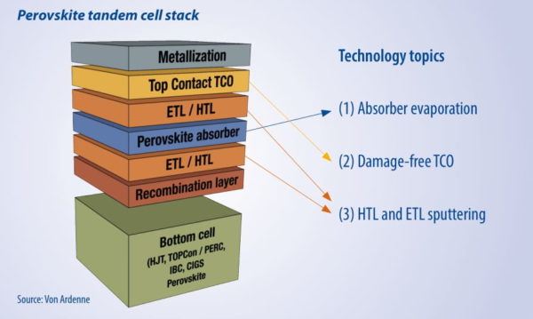
If you look at a basic structure in a tandem device, there is always the bottom cell, which can be HJT, TOPCon [tunnel oxide passivated contact] PERC, or even IBC. And then there are thin film technologies. On top of the bottom cell there is a recombination layer, then the so-called electron (ETL) or hole (HTL) transport layer – depending whether it is a n-type or p-type solar cell. On top of the ETL or HTL is the perovskite layer, then the ETL or HTL again, the TCO [transparent conductive oxide], and the metallisation.
We consider the layers on top of the absorber, such as the ETL or HTL and TCO layer being critical because they must not damage the layers below – and this is something we are working on. We call the process “damage free deposition” coating. Another challenge for tandem devices, we consider, is the absorber itself. There it depends on whether you apply a technology like evaporation or maybe a wet chemistry process, or maybe a hybrid approach. There are also question marks for R&D. With the ETL and HTL layer, what must be found is processes that are scalable – it doesn’t make sense to have high efficiency cells with very low throughputs. We consider sputtering, which is a proven technology for high volume manufacturing, and is a very hot candidate for applying ETL and HTL layers.
And then for the absorption layer, for the perovskite itself, sputtering most probably is not an option. It could be a co-evaporation process where you apply different materials for effective absorption of the blue light.
If you were to apply sputtering or evaporation processes in this way, how would you describe the process flow?
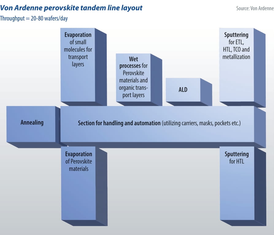
You need the recombination layer, the ETL layer, the perovskite layer, the HTL layer, the top TCO, so between five and eight layers to be applied in a tandem structure – on top of the bottom cell technology. Looking both at capex and opex, we believe it doesn’t make sense to apply eight different pieces of equipment and then the handling. A process flow must be defined where two or three layers, or even four, can be combined in one system. At the end then there are two or three deposition systems, additionally to the standard PERC or HJT or TOPCon processes.
What processes can be combined?
What we see as an ITO based recombination layer, and then the ETL or HTL, from our point of view it is quite reasonable to do in a sputtering system. The perovskite can be deposited through evaporation or wet chemistry – so either through a vacuum system or a wet chemistry process. And then the ETL and TCO on top and there we consider it is quite reasonable to apply it in a sputtering system, where we have platforms today that deliver 10,000 wafer per hour throughput, based on M6, or even platforms going over 1 GW per system of productivity. From these basic five layers, it can result in three systems.
What can you tell me about the latest Von Ardenne platforms?
As I said, we have the R&D tool that has a lot of flexibility in terms of technologies and also in terms of materials that you can apply. There you have a platform where you apply evaporation processes, sputtering processes, and also ALD [atomic layer deposition] processes, and the interface with wet chemistry processes. Heating and annealing stations are also included, in between. This can allow R&D engineers to play around with different technologies and different materials in order to find a nice process flow. However, even at this stage we apply technologies that are scalable. With ALD we see big challenges to GW scale, however a lot of R&D record cells are done, on a very small scale, on ALD processes – or at least part of it. Because of this we have the ALD in the R&D phase in order to just transfer the record efficiencies from square centimetre to the wafer size, in order to find reference processes.
Our customers are developing processes where the ALD can be replaced by sputtering. If a good process flow with sputtering and evaporation only is found, then we are sure we can scale this technology further – because we have already scaled evaporation and sputtering to gigawatt scale. For the pilot tool, our customers already know the process flow and the sequence, but maybe process variations such as deposition rates, temperature, productivity, etc., have to be optimised. But the pilot systems are typically in-line systems where it’s possible to deposit one process sequence. Whereas with the R&D system it is possible to change the process flow and sequence, in the pilot system it is already clearer what direction will be pursued. And the final variations can work towards getting the efficiency and stability. But the basic materials are already defined.
Once defined criteria have been passed on the pilot tool, we can then take this directly and apply it to the gigawatt-scale tool, like the XEANova, which is already well known.
SunPower and First Solar recently announced that they are collaborating on tandem structures. This isn’t a crystalline-perovskite tandem, but likely crystalline silicon from SunPower and cadmium telluride (CdTe) thin film. What do you make of this?
It seems they want to combine classical thin-film technologies together with silicon. And I understand they will bring this together into production next year. We consider this a tandem, where sputtering and evaporation plays a role.
Would that be an IBC-CdTe tandem?
I don’t want to comment too much, but just talking about physics the silicon is effective in the infra-red and visible range, and the CdTe is effective with the higher bandgap, in the blue range. So, in the theoretical limits it really is the perfect fit and a very interesting approach, besides perovskites.
This content is protected by copyright and may not be reused. If you want to cooperate with us and would like to reuse some of our content, please contact: editors@pv-magazine.com.


1 comment
By submitting this form you agree to pv magazine using your data for the purposes of publishing your comment.
Your personal data will only be disclosed or otherwise transmitted to third parties for the purposes of spam filtering or if this is necessary for technical maintenance of the website. Any other transfer to third parties will not take place unless this is justified on the basis of applicable data protection regulations or if pv magazine is legally obliged to do so.
You may revoke this consent at any time with effect for the future, in which case your personal data will be deleted immediately. Otherwise, your data will be deleted if pv magazine has processed your request or the purpose of data storage is fulfilled.
Further information on data privacy can be found in our Data Protection Policy.