From pv magazine Global
String inverters based on gallium nitride (GaN) semiconductors could represent a valid alternative to devices based on silicon (Si) or silicon carbide (SiC) in the future if the industry manages to reduce their size. A consortium led by Fraunhofer Institute for Energy Economics and Energy System Technology IEE is now coordinating a research project to assess how components of GaN inverters can be further miniaturised, in order to achieve lower production costs.
“The aim behind the usage of GaN for power electronic inverters is not primarily focused on efficiency improvements,” Sebastian Sprunck, group leader for components and measuring systems at Fraunhofer IEE, told pv magazine. “Si and SiC-based converters, already reach or exceed 98 % efficiency in certain applications and improving on those values may be possible from a technology point-of-view, but is rarely economically feasible.”
He said the primary goal when using GaN in power electronics is usually the optimisation and miniaturisation of the entire inverter device, including passive components such as cooling systems, casings, and mounting structures.
“When components are miniaturised through this approach, we can potentially harness benefits such as lower material consumption and costs, as well as lighter products, which would reduce costs and efforts required for packaging, delivery and installation,” Sprunck said. “We’re amongst the first research projects to apply GaN to high-power solar inverters, therefore we can only extrapolate possibilities which we need to validate over the course of our project.”
The achievable size reduction is dependent on several parameters and is subject to ongoing study.
“In general, we’re hoping on similar reduction factors that were demonstrated with SiC in comparison to Si technology, only now comparing GaN with SiC. However, it is not possible to directly compare such factors across differing power and/or voltage classes,” Sprunck explained. “Some preliminary results for the power inductors of the GaN-HighPower project are already available and we are now evaluating them.”
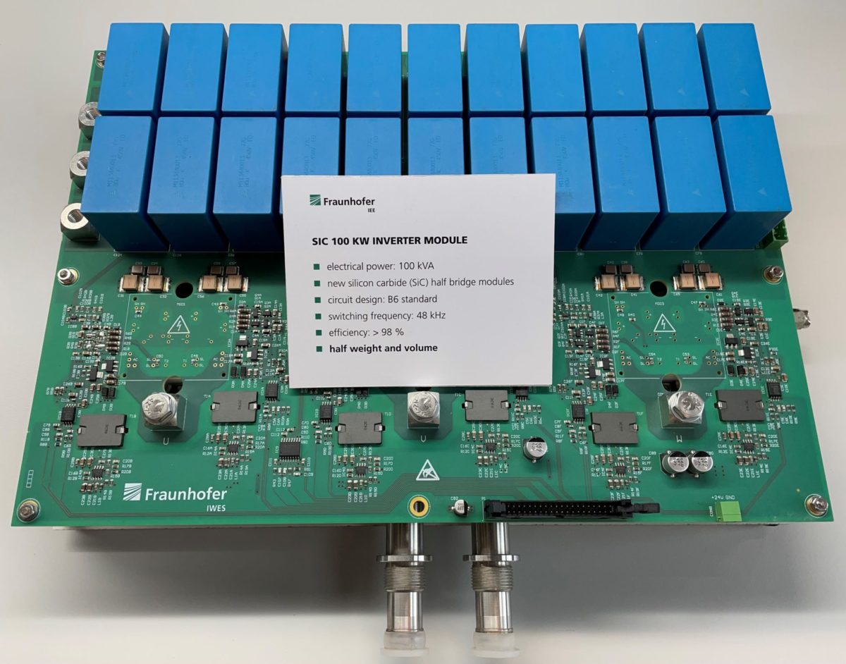
The consortium is now developing its first GaN inverter prototype. It aims to test it in late 2022 or early 2023, with a more integrated demonstrator planned for late 2023. The project aims at converter powers above 100 kVA.
Sprunck noted that GaN is already under investigation in several lower-power applications.
“High power applications such as industrial PV projects of over 100 kW are not typical for GaN, at least not in the short term and it’s currently a challenge to apply these devices to such high power converters, which is one of the reasons we’re conducting this project in the first place,” he said.
The use of gallium nitride in inverters could also allow for higher switching frequencies and smaller passive components such as power inductors or capacitors, which are often the largest, heaviest components in power converters.
“If they can be miniaturised, then often the inverter case can be as well,” Sprunck said. “Other projects utilising GaN power semiconductors in lower-power applications have shown that these effects can lead to lower manufacturing costs. One of the tasks of this project is to investigate if these effects can also be harnessed for high-power applications.”
Infineon Technologies, SMA Solar Technology, and Vacuumschmelze (VAC) also participated in the research project. In addition, the Bonn-Rhein-Sieg University of Applied Sciences is preparing the integration of new components into a technology demonstrator, while TH Köln University of Applied Sciences is helping with the design and optimisation of power electronic inductors.
This content is protected by copyright and may not be reused. If you want to cooperate with us and would like to reuse some of our content, please contact: editors@pv-magazine.com.


By submitting this form you agree to pv magazine using your data for the purposes of publishing your comment.
Your personal data will only be disclosed or otherwise transmitted to third parties for the purposes of spam filtering or if this is necessary for technical maintenance of the website. Any other transfer to third parties will not take place unless this is justified on the basis of applicable data protection regulations or if pv magazine is legally obliged to do so.
You may revoke this consent at any time with effect for the future, in which case your personal data will be deleted immediately. Otherwise, your data will be deleted if pv magazine has processed your request or the purpose of data storage is fulfilled.
Further information on data privacy can be found in our Data Protection Policy.