From pv magazine Global
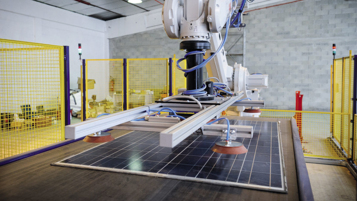
As the solar industry comes of age, dealing with the growing volume of products reaching end of life is already a research priority at universities and institutes the world over. Many different approaches are on trial, though experts are waiting until later this decade when the volume of products is expected to grow significantly, giving them room to experiment with processes at large scale.
Processing and purifying silicon from end-of-life cells back to a state where it can again be inserted back into the PV supply chain to make new cells has proven a major challenge here. It requires high levels of energy and a complex understanding of tiny impurities left in the recycled silicon that differ from brand new material.
Some already say that diverting this silicon to applications with lower purity requirements is the best solution. However, a group of scientists led by the Key Laboratory of Urban Pollutant Conversion at the Chinese Academy of Sciences may have come up with an alternative – one that cuts out the energy-intensive ingot production stage entirely.
“Skipping the process of Si ingot production and wafer cutting can save approximately 40% of the cost of PV module production,” the group explained in its research. “Nonetheless, there is still a major challenge for the current technologies: regenerated solar cells from recovered Si wafers tend to exhibit a decreased conversion efficiency, which is not acceptable for the current competitive PV market.”
Recovery and upgrade
With this in mind, the group sought ways to recover silicon wafers suitable for production of high efficiency cells and modules. They demonstrated a series of chemical treatments that are shown to both purify wafers and improve their surface characteristics, making them suitable for use in new, high-efficiency cells. The process is described in full in “A systematically integrated recycling and upgrading technology for waste crystalline silicon photovoltaic module,” which was recently published in Resources, Conservation and Recycling.
The group took advantage of a process previously used by wafer manufacturers to reduce surface reflectivity and produce “black silicon” wafers.
“Through this technology, desirable and highly pure Si wafers with intact structure, minimally reduced thickness and excellent light-trapping ability are successfully obtained,” the group explained. “The properties of the reclaimed Si wafers are characterised and evaluated for new solar cell manufacturing and packaging, which encourages regenerated solar cells with higher power conversion efficiency than that of new commercial solar cells.”
This content is protected by copyright and may not be reused. If you want to cooperate with us and would like to reuse some of our content, please contact: editors@pv-magazine.com.


Sounds like a great idea. I always was wondering what they are going to do with the huge amount of old solar panels when they stop function…