From pv magazine Global
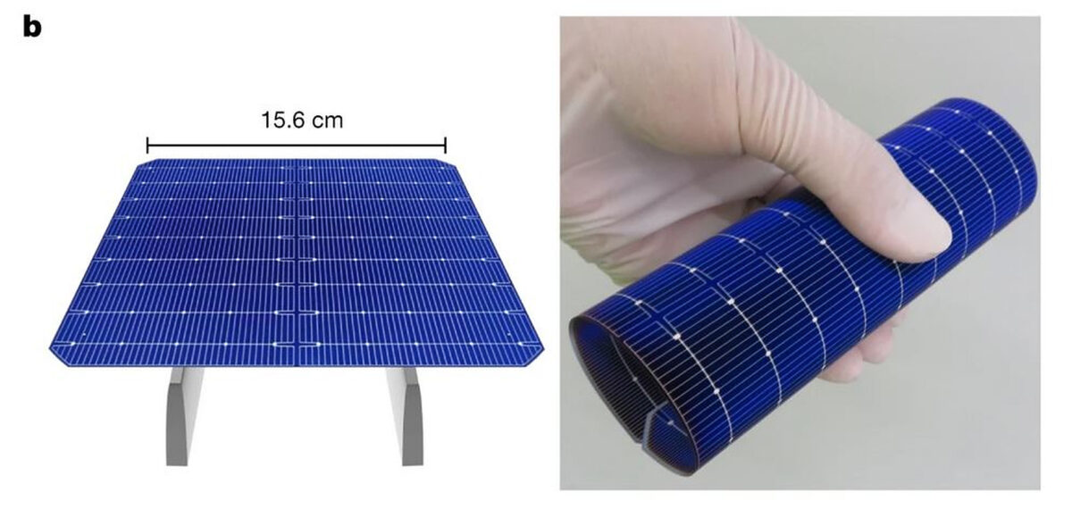
Researchers at the Chinese Academy of Sciences have successfully created foldable crystalline silicon (c-Si) wafers, known for their strong light-harvesting capability, for use in flexible silicon heterojunction (HJT) solar cells.
The scientists said HJT cell technology is ideal for making flexible solar cells, as it eliminates edge warping caused by inner stress during the firing process. The wafers were developed with blunting treatment, a technique commonly used to round a wafer’s edges, in order to prevent chipping and cracking during processing. The researchers said that the treatment resulted in a transition of the fracture mechanism from intrinsic brittle cleavage fracture to shear banding with steps and cracks.
The research team used 180 μm Czochralski n-type c-Si wafers, supplied by China-based Sichuan Yongxiang, to create textured wafers with a thickness of 60 μm.
“The wafers were textured in a 2.1-vol% alkali water solution at 80 C for 10 min to form microscale pyramids on the surfaces,” it explained. “All wafers were cleaned using a standard root cause analysis (RCA) process to remove organics and metal ions. Next, they underwent cleaning in 2.0% hydrofluoric acid water solution for 3 min to etch the surface oxide.”
The academics used the wafers to produce two HJT cells with thicknesses of 65 μm and 55 μm. The first cell had a power conversion efficiency of 23.31%, an open-circuit voltage of 0.752 V, a short-circuit current density of 0.09 mA cm−2, and a fill factor of 82.40%. The second cell hit an efficiency of 23.35%, an open-circuit voltage of 0.754 V, a short-circuit current density of 0.11 mA cm−2, and a fill factor of 82.51%.
The group then applied an anti-reflective coating based on magnesium fluoride (MgF2) on the cells and their efficiency was raised to 24.50%.
“Although this value was lower than that (25.83%) of a thick cell because it was affected by the inferior light-harvesting ability of the thinner wafer, it was a remarkable efficiency compared with that of the current flexible solar cells fabricated from other cost-effective materials,” the scientists said, noting that the use of a 60-μm wafer could reduce production costs by approximately 29%. “Overall, the flexible technology developed in this study reduced the levelised cost of energy by approximately 39% (23%) at the solar cell (module) level.”
The academics presented the new manufacturing process in “Flexible solar cells based on foldable silicon wafers with blunted edges,” which was recently published in Nature. The research group includes scientists from China’s Tongwei (TW), the Changsha University of Science and Technology, Southwest Petroleum University, Soochow University, and Beihang University.
This content is protected by copyright and may not be reused. If you want to cooperate with us and would like to reuse some of our content, please contact: editors@pv-magazine.com.


By submitting this form you agree to pv magazine using your data for the purposes of publishing your comment.
Your personal data will only be disclosed or otherwise transmitted to third parties for the purposes of spam filtering or if this is necessary for technical maintenance of the website. Any other transfer to third parties will not take place unless this is justified on the basis of applicable data protection regulations or if pv magazine is legally obliged to do so.
You may revoke this consent at any time with effect for the future, in which case your personal data will be deleted immediately. Otherwise, your data will be deleted if pv magazine has processed your request or the purpose of data storage is fulfilled.
Further information on data privacy can be found in our Data Protection Policy.