From pv magazine Global
A review of indoor PV cell technologies by an international research team documents more than 250 large area and small area commercial and laboratory devices. It covers organic, dye-sensitised, and perovskite devices, as well as crystalline and amorphous silicon, III-V semiconductor, chalcogenide, and emerging lead-free alternative cells.
“We observed that the interest in the field was really taking off, so we believed a comprehensive review on all indoor PV technologies was due,” the review’s co-author Giulia Lucarelli told pv magazine.
The review also includes a discussion about applications, recent progress, and strategies used to design more stable, highly efficient cells that operate at very low light levels.
“We have provided the performance details of the indoor PV devices at 200 lx and 1000 lx illuminance,” corresponding author, Thomas Brown, told pv magazine, explaining that most homes have a 200 lx illuminance, whereas 1000 lx is typical in very well-lit environments like supermarkets.
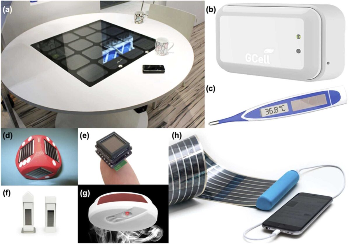
Brown pointed out that one of the initial high-volume market niches for indoor PV has been electronic supermarket shelf labels. Other applications are emerging, such as Internet-of-Things products, where PV is seen as enabling a “fit and forget” approach, where a product is installed once with no further maintenance required. “Think of applying a temperature or other type of sensor in your home and leaving it there to operate without ever having to replace batteries,” said Brown.
Cell technologies covered in the review range from crystalline and amorphous silicon to III-V semiconductor and chalcogenide devices, as well as organic, dye-sensitised, perovskite, and lead-free alternative devices.
Looking at the power conversion efficiency (PCE) and maximum power density (MPD) the team made several observations. For example, it said that it was “obvious that irrespective of the indoor lamp type or intensity”, perovskite solar cells have “outdone” other PV technologies both in terms of efficiency and output power.
The team observed that organic photovoltaic devices (OPV) performed well under light-emitting diodes (LED), while dye-sensitised solar cells (DSSC) outperformed in fluorescent light (FL). But it also cautioned there was only a limited number of reports making it “difficult” to draw any conclusions.
“Among the established technologies, compound and thin-film semiconductors in recent years have shown considerable improvement in performance, with the former delivering high efficiency and output power,” stressed the team. “The lead-free alternatives have just entered the indoor PV arena and have managed to deliver the highest efficiency of around 18 % with a tin-based perovskite.”
Standards for performance reporting were discussed, particularly the need for a protocol for measurement in standard light source spectrum and a standard illuminance level, or levels. “The most utilised currently are 200 lx and 1000 lx so both should continue to be reported,” said the scientists.
They explained that MPD reporting for 200 lx and 1000 lx illuminance is important for product developers designing energy harvesting solutions and products that operate in a range of lighting conditions. “MPD is a more immediate metric since product developers who wish to integrate PV in their items know exactly what is coming out of the PV device,” co-author Abhisek Chakraborty told pv magazine.
Brown added that indoor lamp spectra are diverse, ranging from LED, to compact fluorescent and lamp bulbs with different color temperatures. “We only have 1 sun but a myriad of indoor light sources,” he said.
They also noted that whereas crystalline silicon, thin film, and new PV technologies have stability protocols for outdoor applications, and accelerated stress tests, these are “still lacking” for PV-designed indoor environments only.
In summarising the findings, the team noted indoor laboratory efficiencies for emerging PV technologies are reaching efficiencies in the range of 35 – 45 % under 200 lx and 1000 lx. “The corresponding electrical power densities are in the range of 20 – 25 μW cm-2 at 200 lx and the range of 120 – 150 μW cm2 at 1000 lx illuminance,” it said.
There is work to do in indoor PV stability and more investigation under continuous indoor illumination, noted the team, pointing out that improvements can be achieved “through the right choice of materials, device design and scalable manufacturing” processes.
“The goal is to improve performance while increasing stability and reducing the cost of not only the indoor devices but their integration capabilities with the electronic products they aim to power,” it said.
“As mentioned earlier there is a question of different reporting, illumination, and measurement conditions for indoor PV,” Brown said, referring to the future direction of the research. “We are trying to present some best practices for this. We are also working on some national projects related to developing perovskite PV indoors via more sustainable materials and fabrication processes.”
The review appears in “Photovoltaics for Indoor Energy Harvesting,” published by Nano Energy. The researchers were from Italy’s Tor Vergata University, the Netherlands Organization for Applied Scientific Research (TNO), the Fundación Escuela Tecnologica in Colombia, and Jain University in India.
This content is protected by copyright and may not be reused. If you want to cooperate with us and would like to reuse some of our content, please contact: editors@pv-magazine.com.



By submitting this form you agree to pv magazine using your data for the purposes of publishing your comment.
Your personal data will only be disclosed or otherwise transmitted to third parties for the purposes of spam filtering or if this is necessary for technical maintenance of the website. Any other transfer to third parties will not take place unless this is justified on the basis of applicable data protection regulations or if pv magazine is legally obliged to do so.
You may revoke this consent at any time with effect for the future, in which case your personal data will be deleted immediately. Otherwise, your data will be deleted if pv magazine has processed your request or the purpose of data storage is fulfilled.
Further information on data privacy can be found in our Data Protection Policy.