Researchers from the Chungnam National University (CNU) in the Republic of Korea (ROK) have developed a one-step free patterning of graphene, or OFP-G, that results in very low electrical resistance and avoids photolithography and chemical etching damage.
Graphene is a one-atom-thick sheet of carbon atoms arranged in a hexagonal lattice valued for its exceptional transparency, electrical conductivity, and mechanical flexibility, critically requiring preservation of these properties during fabrication processes.
The CNU researcher’s method addresses the limitation of conventional microelectrode fabrication, where lithographic processes easily damage graphene and degrade its electrical performance.
Instead of removing graphene material, the OFP-G method works by selectively modifying its chemical bonds.
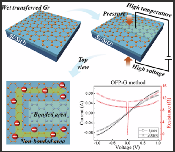
In this process, monolayer graphene transferred onto a silicon dioxide substrate is brought into contact with a pre-etched glass substrate that defines the desired pattern.
The process is carried out under vacuum at 380 °C, where the glass enters a conductive solid-electrolyte state.
When a voltage of 1,000 V is applied, mobile alkali ions migrate within the glass, creating oxygen-rich regions at the graphene interface. These regions locally convert carbon–carbon bonds into carbon–oxygen bonds only in the contact areas, producing a precise stencil-like pattern while leaving the surrounding graphene intact.
Published in the Microsystems & Nanoengineering journal, titled Direct and residue-free patterning of sub-5µm CVD monolayer graphene with highly enhanced conductivity and pattern fidelity, the researchers say the method enables high-resolution patterning of large-area monolayer graphene with feature sizes smaller than 5 micrometres.
The process produces clean, contamination-free graphene surfaces, making it suitable for biosensors, neural interfaces, and flexible transparent electronics, like solar cells.
The researchers found graphene channels fabricated using OFP-G showed resistances as low as 11.5 ohms (5 μm) and 9.4 ohms (20 μm), while conventionally patterned graphene showed negligible conductivity.
CNU School of Mechanical Engineering Professor Wonsuk Jung and research lead, said conventional photolithography inevitably induces graphene damage and delamination at the microscale.
“Our approach achieves exceptionally low electrical resistance and high pattern fidelity, even for fine patterns at the 5 μm scale, without etching-induced defects or chemical contamination,” Jung said.
The researchers believe the technique offers a scalable and reproducible pathway for integrating graphene into flexible, transparent, and bioelectronic devices where surface cleanliness and electrical performance are critical.
“Our approach offers a scalable, reproducible, and contamination-free pathway for patterning high-resolution graphene, and opens new possibilities for the integration of graphene in flexible and transparent electronics,” Jung said.
This content is protected by copyright and may not be reused. If you want to cooperate with us and would like to reuse some of our content, please contact: editors@pv-magazine.com.


By submitting this form you agree to pv magazine using your data for the purposes of publishing your comment.
Your personal data will only be disclosed or otherwise transmitted to third parties for the purposes of spam filtering or if this is necessary for technical maintenance of the website. Any other transfer to third parties will not take place unless this is justified on the basis of applicable data protection regulations or if pv magazine is legally obliged to do so.
You may revoke this consent at any time with effect for the future, in which case your personal data will be deleted immediately. Otherwise, your data will be deleted if pv magazine has processed your request or the purpose of data storage is fulfilled.
Further information on data privacy can be found in our Data Protection Policy.