From the September edition of pv magazine
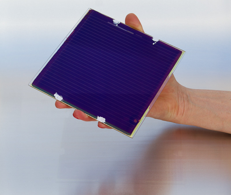
Buyi Yan does not lack self-confidence, as he showed during a recent discussion at SNEC 2019 in Shanghai – and perhaps with good reason. Largely out of view of the Western world, Microquanta Semiconductor – which Yan co-founded four years ago in Hangzhou, China – has set an efficiency record for a perovskite module, and not just with a small laboratory sample. It achieved a 17.25% efficiency rate with a module that was 16 cm long – an impressive scale, as confirmed by external examiners at the Newport PV Laboratory and published in the ongoing efficiency list in Progress in Photovoltaics: Research and Application, a scientific journal.
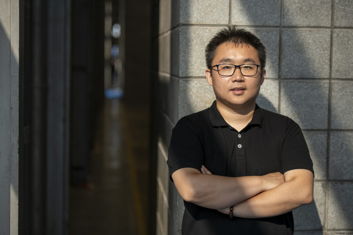
Image: Dave Tacon
Now Yan and his co-founders, Yao Jizhong and Yang Yang, want to take the next step: a multimillion-dollar funding round, quickly followed by a production launch – just like European perovskite startup Oxford PV. And they’re going all in.
The first line is set to come online next year with a capacity of 50-100 MW. Three more lines will follow as the market develops. “Before expanding production, we have to prepare the market for this product,” says Yan. “We need to realize some demonstrations – there will probably be five projects by the end of 2019.”
If this occurs, perovskites will have developed into a product in just 11 years. The material began to attract attention from scientists in 2009, when a team led by Tsutomu Miyasaka at Toin University in Yokohama, Japan, achieved 3.8% efficiency with a perovskite cell. After that came rapid advances; first in efficiency, then stability, and now in production. But there are questions as to whether this pace has been too rapid, and the young technology still has challenges to face.
Learning from experience
Even when half the industry is caught up in technology fever, its assessments can often be wrong. At the end of the last decade, countless thin film silicon factories were built, amid hype that it was the technology of the future. Today, virtually all of them have ceased production, as the modules were far too expensive.
Yan believes such a failure will not be repeated with perovskite. The thin film technologies that survived, such as cadmium telluride, have managed to keep pace with the cost reductions of crystalline silicon. The less fortunate ones could not keep up, because the efficiency increases were too low and they used expensive materials.
“Perovskite was born with a much lower materials cost, unmatched by crystalline silicon, because of the way the materials are synthesized and processed,” Yan says.
Another lesson he has drawn from thin film solar is that “good PV technology must not stay in the lab for too long until it’s just right, it needs to hit the market once the major pieces are in place.” And he believes that this is now the case.
In the end, production costs are crucial, of course. But Yan is reluctant to venture a public statement on this. “The figure depends a lot on production capacity,” he says. “We don’t have an accurate number right now because there aren’t enough data from a production line.”
Many other experts are also working to estimate what it will ultimately cost to successively deposit layers of perovskite, conductors and transparent conductive oxides onto glass, then laminate it and then turn it into a workable product. One such individual is Jan Christoph Goldschmidt, head of the Innovative Solar Cell Concepts group at Fraunhofer ISE. He says the estimate depends on a number of assumptions, such as efficiency and service life. “If you could achieve comparable values to a silicon module – that is, 19% efficiency and 25-year service life – a perovskite module would probably be cheaper than a silicon module today,” he says.
Costs currently sit at roughly $30 per square meter, whereas silicon modules cost around $50 per square meter, Goldschmidt adds. The scientists use this unusual metric because, unlike crystalline silicon, the size of perovskite cells is not determined by wafers.
Critical questions
Anyone who makes a serious announcement about setting up perovskite production is asking skeptics to pose two further questions: Is the material stable? And how unfavorable is it that lead is needed in the layers? Microquanta has already subjected 6×6 cm mini modules to damp-heat and thermal-cycle tests, as defined in the IEC61215 standard. “And these mini modules passed each subtest accordingly,” with an efficiency similar to that of the record-setting module, Yan says.
This is indeed a huge step forward compared to the stability findings that scientists were publishing a few years ago. At that time, the cells were simply destroyed by exposure to light. “This view that perovskite solar cells are not particularly stable has been shaped by cells that use methylammonium lead iodide as a perovskite absorber,” says Goldschmidt.
The methylammonium iodide is very volatile. It evaporates easily, so the corresponding perovskite is a very unstable material. In addition, he notes that the solar cells had a layer of titanium dioxide. If you irradiate that with UV light, it can trigger a chemical reaction.
“Once these two materials are replaced, the solar cells are much more stable,” says Goldschmidt. In addition, the electrode layers, transparent conductive oxides, and buffer layers protect the cell from the surrounding air and oxygen. So it looks as though the stability problem can be solved.
However, damp-heat and thermal-cycle tests are not the only challenges. In the end, products have to pass all of the tests of the IEC standard, while possibly accounting for new degradation mechanisms. Philippe Holzhey and Michael Saliba looked at the situation last year in an article in the Journal of Materials Chemistry. There are promising results for thermal-cycling, damp-heat, outdoor and UV-light tests, they write, but little work has been done on mechanical, reverse bias, high-voltage and humidity-freeze stability.
Lead content
Yan also wants to dispel concerns about the technology, since most of today’s perovskite modules contain lead. “I think it is normal for people outside of the field to regard lead as a point of concern, and I think that people working in this field have an obligation to explain why such concern is misplaced,” says Yan. After all, it only gets into the environment if modules are not properly recycled at the end of their service life. Yan also notes that the perovskite layers are thin, with less than 400 mg of lead per square meter of module. He claims this is significantly less than levels in soil, if one considers a square-meter layer.
This is confirmed in principle by Helmer Schack-Kirchner, a soil ecologist at the University of Freiburg. One square meter of the upper 25 cm soil layer consists of roughly 375 kg of dry matter. If we assume that a perovskite module is not recycled, the encapsulation is destroyed and water washes out the lead, a concentration of 1.1 mg/kg would be added to the topsoil. According to the Geochemical Atlas of Europe, this is 20 times less than the 22.6 mg/kg found on average in the 843 soil samples examined for this purpose across Europe. It’s also below the 3-6 mg reported in the atlas for sparsely populated areas. It is also just a tenth of the threshold value for sandbox sand in Germany, which is subject to the most stringent requirements.
So is the lead harmless? Well, not exactly. Keeping lead content as low as possible is a generally accepted goal, and therefore the element may only be contained in products under the European RoHS Directive with special approval. And there are silicon modules that do not contain lead. Whether and where lead is acceptable in new technologies ultimately will be a socio-political decision that balances the advantages of a cheaper energy supply and perhaps a faster energy transition against the disadvantages that could arise in the event that the modules are not disposed of properly.
“Scientists are therefore not in a position to answer the question of whether lead should be accepted in this application,” says Schack-Kirchner.
Early days
Microquanta Semiconductor can hold its own when it comes to startup stories. Yan says he and his two co-founders, who met while studying at Zhejiang University in Hangzhou, recognized the potential of perovskites as early as 2012. At the time, Yan was doing his master’s degree at King Abdullah University of Science and Technology on quantum dot applications in photovoltaics, while Yao Jizhong was at Imperial College in London, working on organic and hybrid solar cells. “I called Yao and said, ‘let’s start something’,” Yan recalls. The local government of Hangzhou liked the idea and helped them with a startup program, by providing the company’s first office and introducing them to potential investors. Yang Yang later returned from his Ph.D. at UCLA, became a professor at Zhejiang University, and joined the group.
They officially founded Microquanta Semiconductors in 2015. Two years later, Insigma – an incubator that also emerged from the university – entered the market with CNY 60 million ($8.5 million) of funding. The money that will now go into setting up production facilities comes from Three Gorges Capital. Yan has estimated the total at tens of millions of yuan.
From the outset, Microquanta has relied on inkjet printing technology, not only for the perovskite layer, but for as many of the layers that make up the cell as possible. “Because these layers are not independent, the device architecture, including all layers, is regarded as an important focus of our R&D efforts,” says Yan. He considers printing technologies particularly cost-effective. Since they print at temperatures below 200 degrees Celsius, capital and operating costs are lower than with the vacuum-coating technologies used by other companies. Although the substances are more exposed to environmental factors during printing, they have been tried and tested in other industries. Microquanta Semiconductor currently prints on an area of 30×40 cm. On the production line, the size will be increased to one square meter.
To transform the coated surface into a module, the coating is separated into parts which are then interconnected, as with other thin-film technologies. The process is known as monolithic interconnection. The record-setting module consists of seven cells. But at 17.25% efficiency, the full potential has not yet been tapped, says Yan. “There is still plenty of room for improvement.”
Those who think all this is just a pipe dream for perovskite afficionados would be mistaken. A number of crystalline silicon cell manufacturers are interested in the technology or are already actively working on it. They are motivated by the prospect of being able to make further advances once all the other improvements planned for silicon have been exhausted in a few years’ time.
This content is protected by copyright and may not be reused. If you want to cooperate with us and would like to reuse some of our content, please contact: editors@pv-magazine.com.


“Even when half the industry is caught up in technology fever, its assessments can often be wrong. At the end of the last decade, countless thin film silicon factories were built, amid hype that it was the technology of the future. Today, virtually all of them have ceased production, as the modules were far too expensive.”
Different tools were developed and manufacturing processes have allowed larger cells to be produced using mono-crystalline PV cells. There is a cost and panel size for consistency that will be the sweet spot for incorporation in small as well as large solar PV installations. This push for manufacturing begs the question, if perovskites can be made this efficient, then could one add a process to an already functioning manufacturing line and spray on a perovskite coating on standard mono-crystalline solar cells creating a tandem cell with efficiencies over 30%? Same sized solar PV panels, on average 20 square feet, 1.86 square meters, with the solar PV harvest of 30 to 35% of the solar insolence falling on the panel each day. Bring it on!