From pv magazine Global
Standalone perovskite solar cells have made rapid progress in terms of efficiency, with several research devices performing at 25% or better. Many of the best performing devices to date have utilised an n-type, or n-i-p, cell architecture for the perovskite layer.
When it comes to fabricating tandem devices that combine perovskites with a silicon bottom cell, however, the n-i-p architecture comes up against major challenges and many researchers have instead chosen to focus on the p-i-n architecture, with the unfortunate side effect of cutting tandem devices out from some of the most promising research in perovskites.
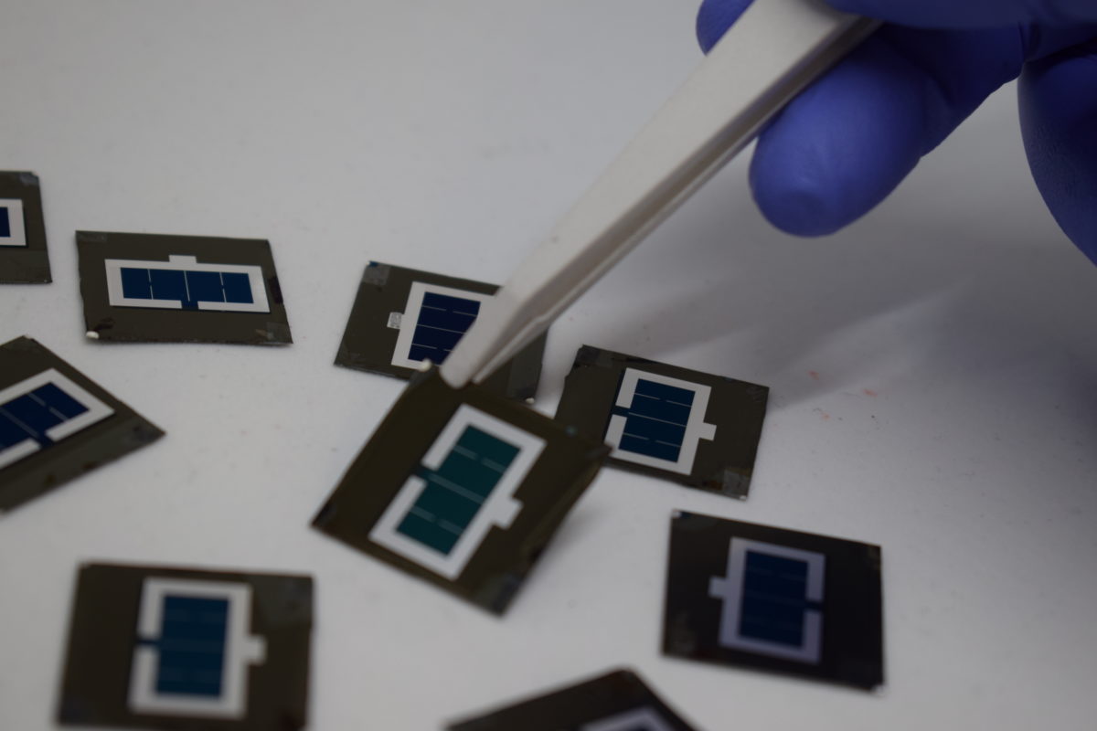
Scientists led by Saudi Arabia’s King Abdullah University of Science and Technology (KAUST), however, were able to overcome several of these challenges. They demonstrated a tandem cell based on an n-i-p perovskite stacked on top of a silicon heterojunction cell that achieved 27% efficiency. This represents a big jump from the previous record of 22%.
The device is described in the paper Ligand-bridged charge extraction and enhanced quantum efficiency enable efficient n–i–p perovskite/silicon tandem solar cells, published in Energy & Environmental Science. The group worked with a layer of a material called amorphous niobium oxide, creating selective contacts that limited the amount of light energy absorbed by the cell but lost as heat.
“Overall, we allowed more light to be captured in the regular structured tandem solar cells, and we converted the absorbed to energy more effectively thanks to our newly developed contacting materials,” explains KAUST researcher Erkan Adin. “With these advancements, we achieved a power conversion efficiency exceeding 27%.”
Having overcome these fundamental challenges, the group soon expects to reach even higher efficiencies with the n-i-p tandem cell technology, also noting that its sees strong potential for use of the cells in solar-driven water splitting for hydrogen production. And the next step for the group will be to scale the devices up to work on ‘full size’ six inch silicon wafers. “At KAUST, we are working to scale up this platform towards the industrial standards of the silicon technology, namely six inches wafers,” Stefaan de Wolf, a leader of the research team, said. “We already develop our tandem technologies on double-side textured SHJ cells, which is today’s industry standards.”
This content is protected by copyright and may not be reused. If you want to cooperate with us and would like to reuse some of our content, please contact: editors@pv-magazine.com.


By submitting this form you agree to pv magazine using your data for the purposes of publishing your comment.
Your personal data will only be disclosed or otherwise transmitted to third parties for the purposes of spam filtering or if this is necessary for technical maintenance of the website. Any other transfer to third parties will not take place unless this is justified on the basis of applicable data protection regulations or if pv magazine is legally obliged to do so.
You may revoke this consent at any time with effect for the future, in which case your personal data will be deleted immediately. Otherwise, your data will be deleted if pv magazine has processed your request or the purpose of data storage is fulfilled.
Further information on data privacy can be found in our Data Protection Policy.