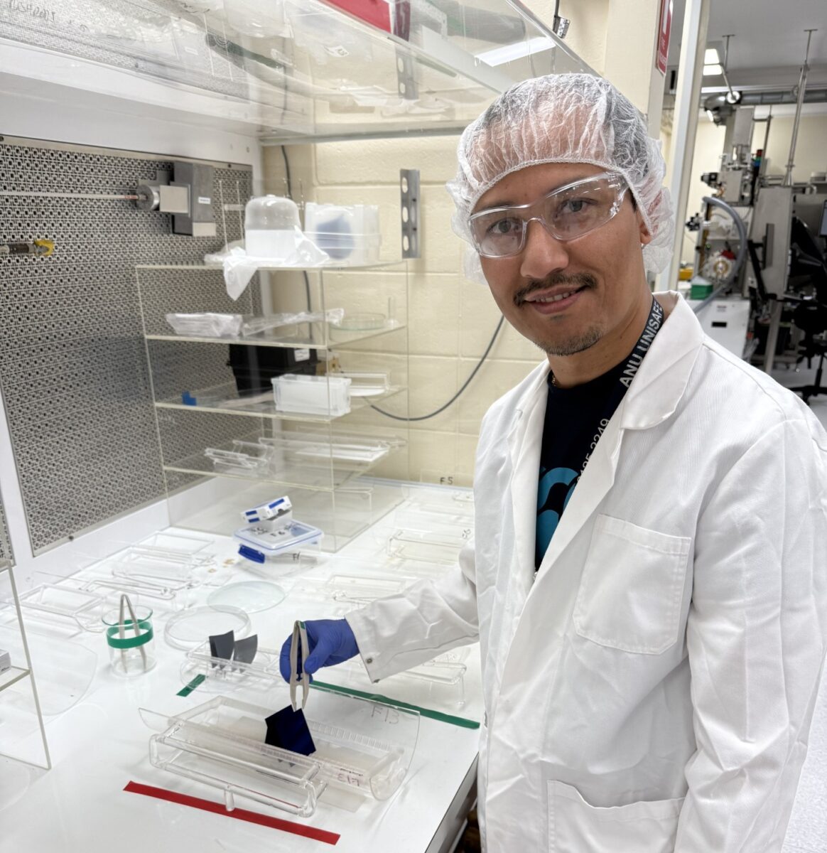
A research team comprising scientists from the Australian National University and Chinese module manufacturer Longi has investigated the resistivity distribution of antimony (Sb)- and phosphorous (P)-doped wafers used in solar cell manufacturing and have found that they offer comparable mechanical strength. However, their work also showed that Sb-doped wafers have a more uniform resistivity, with a slight increase near the tail end.
“Our study elucidated why Sb-doped n-type silicon ingots can achieve uniform resistivity distribution despite antimony’s very low segregation coefficient,” the research’s corresponding author, Rabin Basnet, told pv magazine. “We demonstrated that the key factor is the controlled evaporation rate of Sb during Czochralski growth, not co-doping with phosphorus as often speculated. This finding helps explain how the industry has managed to produce uniform Sb-doped ingots and provides a scientific basis for optimizing doping uniformity in next-generation wafers.”
Currently, antimony appears to be more expensive than phosphorus in terms of raw material costs. However, this higher upfront price does not necessarily translate into a higher total cost for photovoltaic wafers. When considering factors such as manufacturing yield, the overall performance of the wafers, and their long-term reliability, antimony-doped silicon ingots may offer advantages that offset the initial expense.
In their work, presented in “Resistivity distribution and donor properties of antimony-doped n-type Czochralski silicon ingots,” published in Solar Energy Materials and Solar Cells, the scientists explained that they conducted their tests on 182 mm × 182 mm Sb- and P-doped wafers supplied by Longi itself, which has recently introduced antimony doping in its ingot production.
The P-doped and Sb-doped wafers had resistivities of 1 Ω·cm and 0.8 Ω·cm, respectively. Both types were laser-scribed into 30 mm × 50 mm coupons with a comb-like structure. These coupons were then etched in tetramethylammonium hydroxide (TMAH) to remove saw damage and any residuals from laser ablation. After cleaning, a 15 nm-thick aluminium oxide (AlOx) layer was deposited via atomic layer deposition (ALD) at 150 °C, followed by annealing at 400 °C for 30 minutes.
Using the T/CSTM 00587–2023 method, which measures the bending strength of crystalline‑silicon photovoltaic cells via a four‑point bending setup, the research group conducted strength measurements on the M10 wafers. They also employed Electron Paramagnetic Resonance (EPR) spectroscopy to analyse defects and doping levels.
The analysis showed that wafers fabricated from Sb-doped ingots exhibited more uniform resistivity, with a slight increase near the tail end, compared to their P-doped counterparts.
For further analysis, the team utilised EasySpin, a MATLAB toolbox for simulating and fitting EPR spectra, and observed “weaker” hyperfine lines in the Sb-doped wafers, attributed to the presence of Sb atom clusters.
The team noted that, currently, Sb-doped and P-doped wafers offer comparable mechanical performance. The main findings of their work consist of having detected the high resistivity uniformity and the unique EPR signatures of the Sp-doped samples.
“However, ingot yield is expected to increase with Sb doping, leading to significant cost-reduction potential for n-type wafers,” Basnet concluded.
The research team comprised academics from the US Department of Energy’s National Renewable Energy Laboratory (NREL) and Colorado School of Mines (USA).
This content is protected by copyright and may not be reused. If you want to cooperate with us and would like to reuse some of our content, please contact: editors@pv-magazine.com.


By submitting this form you agree to pv magazine using your data for the purposes of publishing your comment.
Your personal data will only be disclosed or otherwise transmitted to third parties for the purposes of spam filtering or if this is necessary for technical maintenance of the website. Any other transfer to third parties will not take place unless this is justified on the basis of applicable data protection regulations or if pv magazine is legally obliged to do so.
You may revoke this consent at any time with effect for the future, in which case your personal data will be deleted immediately. Otherwise, your data will be deleted if pv magazine has processed your request or the purpose of data storage is fulfilled.
Further information on data privacy can be found in our Data Protection Policy.