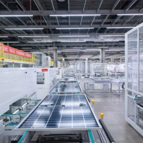
Researchers from Nanyang Technological University (NTU) in Singapore have developed ultrathin perovskite solar cells with absorber layers as thin as just tens of nanometers.
The research work tackles a key challenge in the development of transparent photovoltaics: balancing optical transparency with electrical performance without sacrificing scalability or manufacturability while maintaining minimal instrument safety.
“We push perovskite solar cells to the ultimate thickness limit, demonstrating fully vacuum-processed devices with absorbers down to around 10 nm compared to the conventional 500–700 nm range, making them both efficient and aesthetically beautiful and see-through,” NTU researcher Annalisa Bruno told pv magazine. “This represents a step toward scalable, design-flexible photovoltaic systems suitable for seamless integration into buildings.”
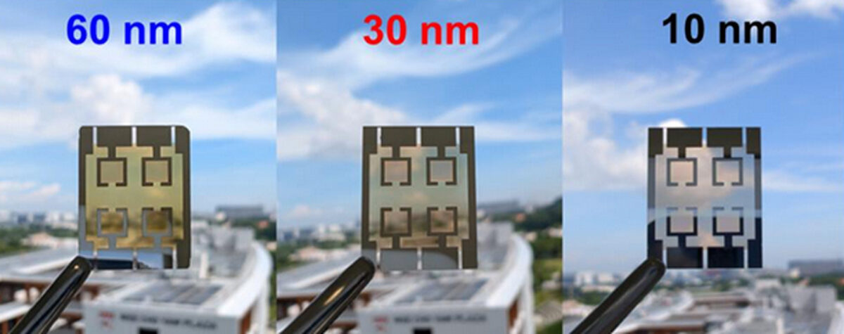
For their experiments, the scientists used planar methylammonium lead iodide (MAPbI3) perovskite films grown on a Spiro-TTB hold transport layer (HTL) and and a self-assembled monolayer (SAM). Film thickness was varied from 10 to 700 nm, with optical studies showing bandgap widening at ultrathin scales due to quantum confinement.
X-ray diffraction (XRD) showed that the film’s composition and crystal orientation change with thickness, improving charge flow in p.i.n. devices. Field emission scanning electron microscopy (FESEM) and atomic force microscopy (AFM) confirmed that the films are smooth, uniform, and stable even at just 10 nm thick.
The perovksite cell design consisted of a substrate made of glass and indium tin oxide (ITO), the Spiro-TTB HTL, the perovskite absorber, a buckminsterfullerene (C60) electron transport layer (ETL), a bathocuproine (BCP) buffer layer, and a silver (Ag) metal contact.
Tested under standard illumination conditions, the cells built with 10 nm, 30 nm, and 60 nm absorbers achieved power conversion efficiencies of 7%, 11%, and 12%, respectively, and they maintained their performances also in the low-illumination regime.
Moreover, the 30 nm and 60 nm devices showed the highest reported light-utilisation efficiency (LUE) for ultrathin devices, indicating a favourable balance between transparency and performance. The 10 nm cell, by contrast, showed reduced open-circuit voltage and some hysteresis, suggesting processing optimisation is needed.
“The 60 nm-thick cell achieved an average visible transparency of about 41% with a power conversion efficiency close to 8%, with a LUE of 3.13. These values of LUE, with further optical engineering, have the potential to reach LUE values above 5%,” said the research lead author Luke White. “All devices exhibited near colour-neutral transparency, with a colour rendering index of 79.7, suggesting compatibility with architectural requirements.”
The cell design was presented in “Ultrathin Fully Vacuum-Processed Perovskite Solar Cells with Absorbers Down to 10 nm,” published in ACS Energy Letters.
“Our findings are particularly relevant for the built environment, which represents a significant share of global energy demand,” said Bruno. “Technologies that enable buildings to generate electricity without altering their appearance are expected to play a central role in the expansion of distributed renewables. Perovskite materials are especially promising in this context, thanks to their tunable optical properties, compatibility with low-temperature processing, and potential for large-area manufacturing.”
This content is protected by copyright and may not be reused. If you want to cooperate with us and would like to reuse some of our content, please contact: editors@pv-magazine.com.


By submitting this form you agree to pv magazine using your data for the purposes of publishing your comment.
Your personal data will only be disclosed or otherwise transmitted to third parties for the purposes of spam filtering or if this is necessary for technical maintenance of the website. Any other transfer to third parties will not take place unless this is justified on the basis of applicable data protection regulations or if pv magazine is legally obliged to do so.
You may revoke this consent at any time with effect for the future, in which case your personal data will be deleted immediately. Otherwise, your data will be deleted if pv magazine has processed your request or the purpose of data storage is fulfilled.
Further information on data privacy can be found in our Data Protection Policy.