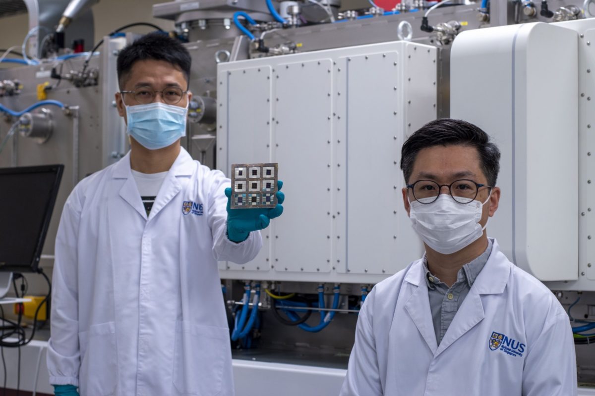
A team of researchers from the National University of Singapore (NUS) claim their solar cells made using perovskite and organic materials have achieved a power conversion efficiency of 23.6%, approaching that of conventional silicon solar PV cells.
Dr Chen Wei, Research Fellow at the NUS Department of Chemical and Biomolecular Engineering, said the achievement is a “significant leap” from the current power conversion rate of about 20% reported by other studies on perovskite/organic tandem solar cells.
“In our latest work, we have demonstrated a power conversion efficiency of 23.6%,” he said. “This is the best performance for this type of solar cell to date.”
Wei said the latest result is approaching the power conversion rate of 26.7% of conventional silicon solar cells, which is the dominating technology in the current solar PV market.
Although perovskite/organic tandem solar cell technology is attractive for next-generation thin-film PV, its efficiency lags behind other types of tandem solar cells featuring stacks of two or more absorber layers.
To address this technological challenge, the NUS research team, in collaboration with scientists from the University of Hong Kong and Southern University of Science and Technology in China, developed an interconnecting layer (ICL) that reduces voltage, optical and electrical losses within the tandem solar cell.
In a paper published in Nature Energy, the research team revealed that the ICL is based on a 4-nanometre-thick sputtered indium zinc oxide layer inserted between organic bathocuproine and molybdenum oxide with enhanced electrical properties and transmittance in the near-infrared region.
Wei said the technology had delivered a maximum efficiency of 23.60% (22.95% certified) in the perovskite/organic tandem solar cell. In addition, the tandem device retained 90% initial efficiency after 500 hours of maximum power point tracking under continuous illumination.
Lead researcher Professor Hou Yi said the technological breakthrough opens the door to thin-film tandem solar cells that are light and flexible.
“Our study shows the great potential of perovskite-based tandem solar cells for future commercial application of photovoltaic technology,” he said. “Building on our new discovery, we hope to further improve the performance of our tandem solar cells and scale up this technology.”
This content is protected by copyright and may not be reused. If you want to cooperate with us and would like to reuse some of our content, please contact: editors@pv-magazine.com.


Efficiency isn’t the major stumbling block with perovskites – longevity is.
“In addition, the tandem device retained 90% initial efficiency after 500 hours of maximum power point tracking under continuous illumination”. Losing 10% of your production every quarter is not a viable business model for any developer. Hopefully, researchers will laser focus on that problem now that they’ve achieved >20% efficiency.
Il Silicio semimetallico possiede 4 elettroni nella sfera elettronica esterna. Se il Silicio purissimo viene drogato con materiali con tre elettroni come il Boro si chiama Si+ o Si(positivo) o Si p. Invece il Silicio drogato con materiali come il Fosforo che possiede 5 elettroni esterni si chiama Si- o Si(negativo) o Si n. Sovrapponendo il Si(p) col Si(n) si ottiene la cosiddetta giunzione p-n. Tale giunzione crea il cosiddetto diodo semiconduttore a giunzione che ha la caratteristica di fare passare la corrente continua in un solo senso . I LED che tutti conoscono sono Diodi semiconduttori che si illuminano emettendo luce colorata quando la corrente continua passa nel verso giusto collegando il positivo al positivo (della batteria) ed il negativo al negativo. Chiaramente la differenza di potenziale deve essere uguale a quella del LED altrimenti il LED si brucia. Quanto qui espresso in modo semplificato implica una tecnologia che ha preso piede negli anni 40-50 e si è sviluppata fino al 2000 circa quando l’efficienza della giunzione ha raggiunto valori prossimi al 20/100. Tuttavia la tecnologia energivora del silicio ha portato gli scienziati ad elaborare altri sistemi meno costosi ed inquinanti per raggiungere lo stesso scopo del Si purissimo. Si è notato che il minerale perowiskite con una formula chimica simile al carbonato di calcio CaCO3 come ad esempio la perowiskite al titanato di bario BaTiO3. Si è notato sperimentalmente che se si sostituisce stechiometricamente l’ossigeno con gruppi organici ed alogeni come ad esempio BaTiO2(CHCl) si ottengono giunzioni con caratteristiche molto simili a quelle derivate dal Si metallico attraverso procedimenti chimici e fisici molto meno costosi e soprattutto meno inquinanti. Si osservi inoltre che la formula scritta sopra “perowiskite sostituita” presenta anche porzioni organiche come i gruppi CH. Questo cambiamento ha reso i semiconduttori molto meno costosi e meno dipendenti dalla chimica inorganica che implicava la produzione del Silicio metallico purissimo. Allo stato attuale le perowiskiti sostituite si stanno facendo strada nella tecnologia a semiconduttore con rendimenti fino al 23/100 cioè superiori al Si. Questa nuova tecnologia sicuramente condurrà a costituire strutture fotovoltaiche meno pesanti e probabilmente forse in meno di 5-10 anni passeremo completamente al POV (fotovoltaico organico) in cui il pannello avrà un peso insignificante e potrebbe essere direttamente stampato sulle tegole o perfino sui muri verticali e vetrate con qualsiasi inclinazione.
Google translated: “Semi-metallic silicon has four electrons in the outer electron sphere. If very pure silicon is doped with materials with three electrons, such as boron, it is called Si+ or Si(positive) or Si p. On the other hand, if silicon is doped with materials such as phosphorus, which has five electrons on the outside, it is called Si- or Si(negative) or Si n. When Si(p) is superimposed on Si(n), the so-called p-n junction is obtained. This junction creates the so-called junction semiconductor diode which has the characteristic of passing direct current in only one direction. The LEDs we all know are semiconductor diodes that light up by emitting coloured light when the DC current passes in the right direction by connecting the positive to the positive (battery) and the negative to the negative. Of course, the potential difference must be equal to that of the LED, otherwise the LED will burn out. What is expressed here in a simplified way implies a technology that took off in the 40s and 50s and developed until about 2000 when the efficiency of the junction reached values close to 20/100. However, the energy-intensive technology of silicon led scientists to devise other less expensive and less polluting systems to achieve the same purpose as pure Si. It has been noted that the mineral perovskite with a chemical formula similar to calcium carbonate CaCO3 such as barium titanate BaTiO3. It has been noted experimentally that if one replaces oxygen stoichiometrically with organic groups and halogens such as BaTiO2(CHCl), one obtains junctions with characteristics very similar to those derived from metallic Si through chemical and physical processes that are much less expensive and above all less polluting. It should also be noted that the formula written above “substituted perovskite” also has organic portions such as CH groups. This change has made semiconductors much less expensive and less dependent on inorganic chemistry, which involved the production of very pure silicon metal. At present, substituted perovskites are making their way into semiconductor technology with yields of up to 23/100, i.e. higher than Si. This new technology will certainly lead to less heavy photovoltaic structures and probably in less than 5-10 years we will switch completely to POV (organic photovoltaics) where the panel will have an insignificant weight and could be directly printed on roof tiles or even on vertical walls and glass at any inclination.”