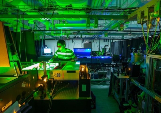
A research team at the University of New South Wales (UNSW) has developed an artificial intelligence-assisted workflow to fast-track the discovery of next-generation semiconductor materials.
“The work tackles a long-standing expensive and time-consuming problem in the field, where researchers have typically made incremental changes to known materials rather than exploring new ones systematically,” the researchers said.
The new AI-assisted workflow targets two-dimensional hybrid perovskites, a class of semiconductor materials used in solar cells and light-emitting diodes (LEDs) that are built by combining inorganic layers with organic molecules.
These organic components play a critical role in determining how the semiconductor material behaves, particularly how it transports electrical charge, but the UNSW team said designing and identifying viable materials currently relies heavily on trial-and-error and expert intuition approaches.
“Small molecular changes can radically alter performance, but with millions of possible combinations, identifying viable candidates is a major bottleneck,” the researchers said, adding that their AI-assisted approach replaces “slow, iterative materials discovery with a targeted, data-driven approach.”
Unlike previous approaches, the team’s system works backwards from a desired outcome, such as how a material should handle electrical charge, to identify molecules that could deliver that result.
Once potential candidates have been identified, the system screens large numbers of them and filters out those that would be impractical to make.
Applied across millions of molecular possibilities, the workflow was able to rapidly narrow the field to a small set of candidates that met the required criteria. These were then checked using detailed simulations to confirm their performance.
While the identified candidates have not yet been validated in the lab, the researchers said the workflow could significantly improve the efficiency of materials discovery.
“The approach could help speed up the development of new materials for electronics and energy technologies by making the search process far more efficient,” they said.
The research paper has been published in the journal Science Advances.
This content is protected by copyright and may not be reused. If you want to cooperate with us and would like to reuse some of our content, please contact: editors@pv-magazine.com.


By submitting this form you agree to pv magazine using your data for the purposes of publishing your comment.
Your personal data will only be disclosed or otherwise transmitted to third parties for the purposes of spam filtering or if this is necessary for technical maintenance of the website. Any other transfer to third parties will not take place unless this is justified on the basis of applicable data protection regulations or if pv magazine is legally obliged to do so.
You may revoke this consent at any time with effect for the future, in which case your personal data will be deleted immediately. Otherwise, your data will be deleted if pv magazine has processed your request or the purpose of data storage is fulfilled.
Further information on data privacy can be found in our Data Protection Policy.